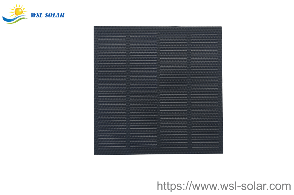
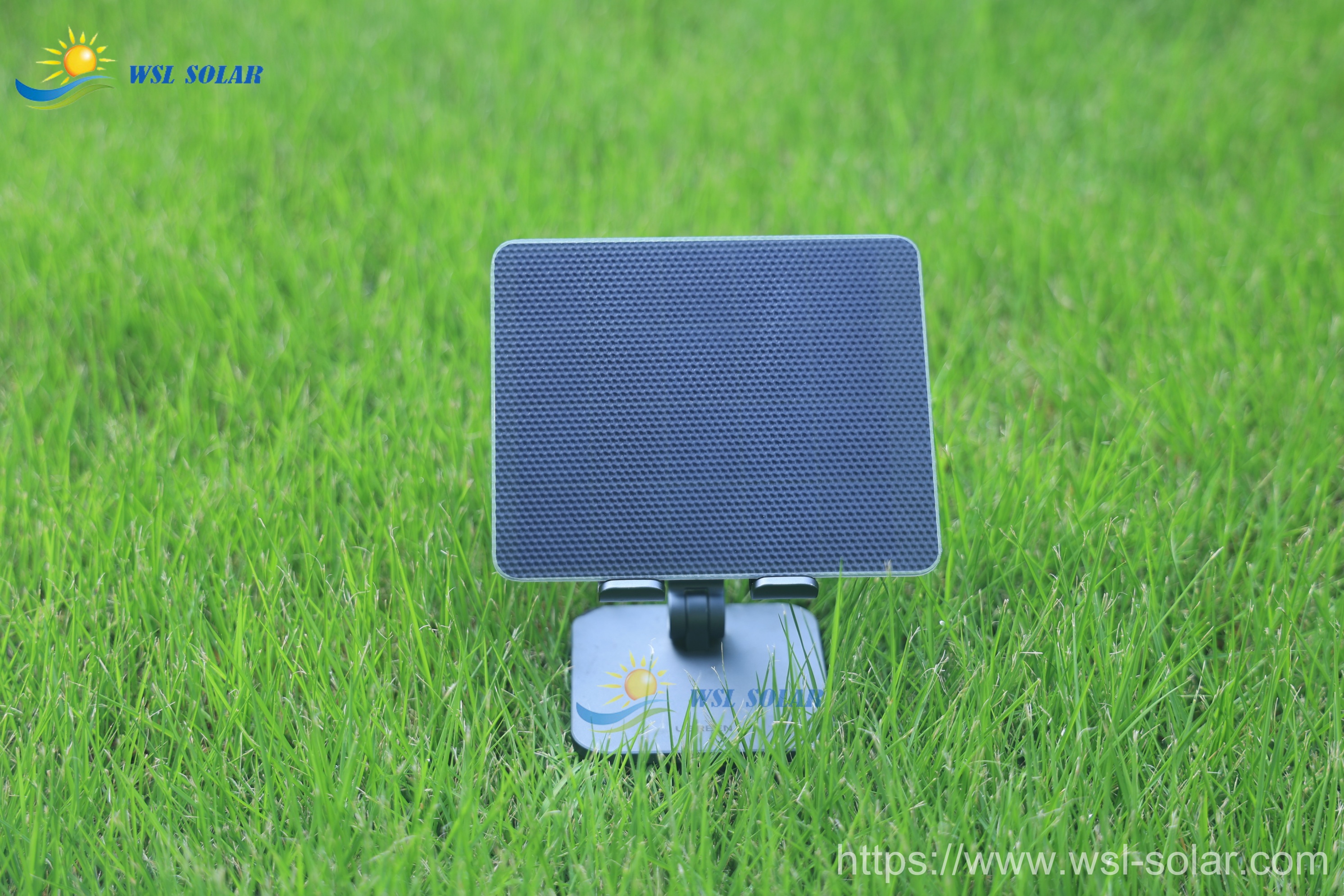
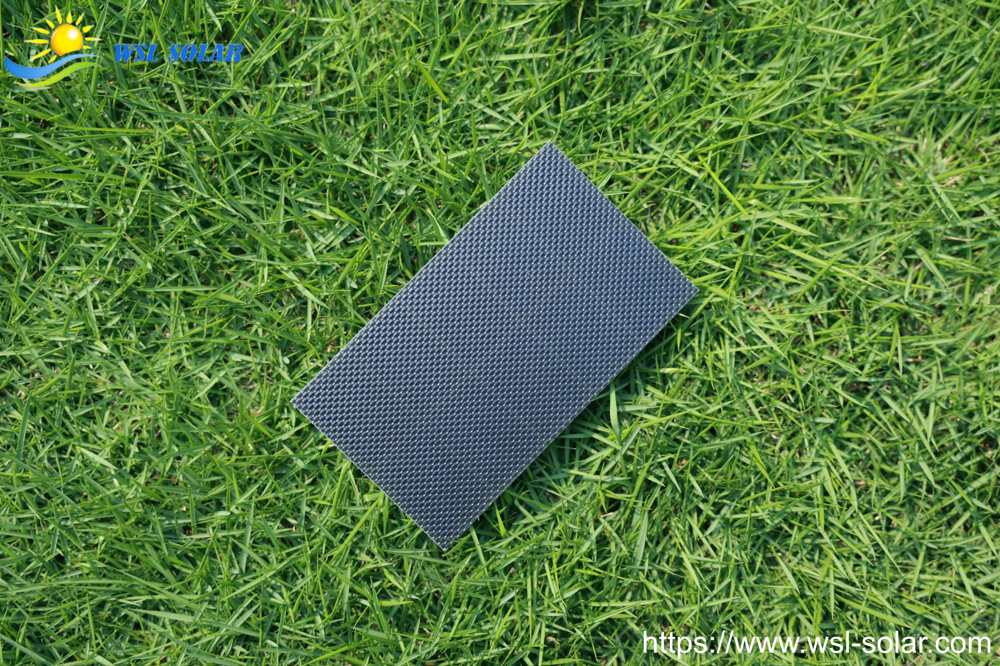
Key Features: – Utilize high efficiency mono solar cell, up to 23% efficiency – Laminated by ETFE film, lightweight, thin and portable – Waterproof, scratch resistant, and UV resistant – Customized solar panels for industrial use
Description: 2V 2W Solar Panel
This 2W solar panel utilizes high efficiency mono PERC solar cells with efficiency up to 23%, to ensure its high output. It is laminated by ETFE film to protect the solar cells inside, making it lightweight, thin and portable. This custom solar panel is waterproof, scratch resistant, and UV resistant, it is ideal for use in off grid applications such as solar powered GPS tracking, educational kits, road studs, solar chargers etc.
Applications: ETFE solar panels are widely used in IoT applications, marine buoys, wireless sensors, GPS devices, asset tracking, solar chargers and educational DIY kits etc.
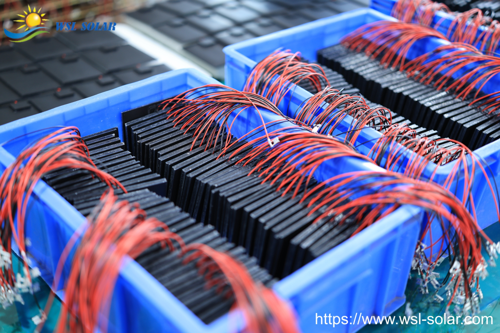
WSL Solar has been a quality and professional manufacturer of custom solar panels, solar mini panels, IoT solar panels and solar solution provider in China since 2006.
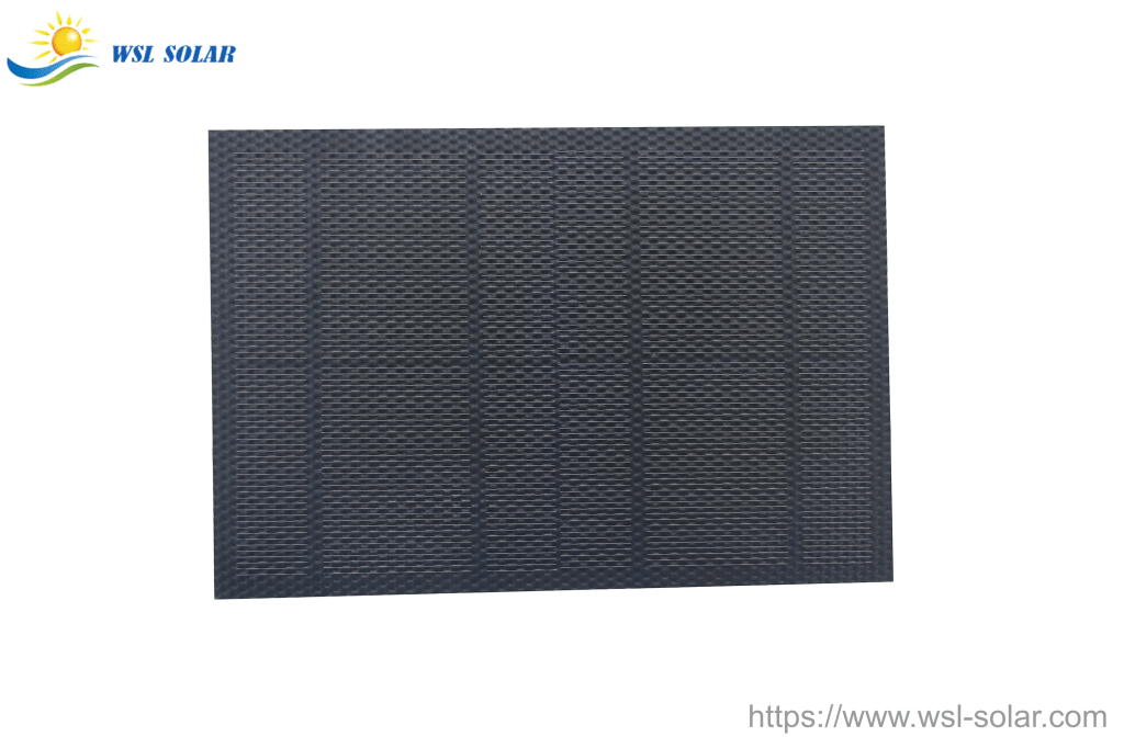
Key Features: – Utilize high efficiency mono solar cell, up to 23% efficiency – Laminated by ETFE film, lightweight, thin and portable – Waterproof, scratch resistant, and UV resistant – Customized solar panels for industrial use
Description: 2V 3W Solar Panel
This 3W solar panel utilizes high efficiency mono PERC solar cells with efficiency up to 23%, to ensure its high output. It is laminated by ETFE film to protect the solar cells inside, making it lightweight, thin and portable. This custom solar panel is waterproof, scratch resistant, and UV resistant, it is ideal for use in off grid applications such as solar powered GPS tracking, educational kits, road studs, solar chargers etc.
Applications: ETFE solar panels are widely used in IoT applications, marine buoys, wireless sensors, GPS devices, asset tracking, solar chargers and educational DIY kits etc.
The pain points in producing custom-made small-sized solar panels (typically referring to those ranging from tens of milliwatts to several watts, used in IoT devices, sensors, consumer electronics, etc.) mainly lie in balancing process, cost, efficiency, and reliability.
Three major pain points
Pain Point 1: The main busbar design (dot/segmented) of mainstream large-size solar cells leads to significant waste during small-size cutting.
Background – Currently, mainstream large-size solar cells (182mm×182mm, 210mm×210mm) generally adopt a multi-busbar (MBB, 9BB~18BB) design with discontinuous “segmented” or “dot” busbar lines to reduce silver loss and improve efficiency.
– There are no metal electrodes between these busbars.
Impact on Small-Size Cutting
– When you cut multiple smaller wafers (e.g., to 20mm×20mm or even smaller) from a large solar cell:
– The smaller wafers are likely to fall into the metal-free areas between the busbar lines, resulting in a lack of complete busbars for soldering or conduction.
– Even if the busbar positions are aligned as much as possible during cutting, it still results in wafer-level layout waste—many areas cannot become effective wafers, and the overall utilization rate may only be 40~60%.
Compared to older solar cells
In the past, small-sized solar cells (such as 156mm or 125mm) mostly had continuous through-type main grid lines. When cutting the cells into smaller pieces, current could be drawn out as long as a section of the main grid was included. This was much more flexible than the current segmented design.
Pain Point 2: Reduced Solar Cell Thickness (220μm → 140μm or even thinner) Leads to a Sharp Drop in Process Yield
Background
– To reduce costs and improve efficiency (thinner cells shorten carrier transport paths and reduce recombination), the mainstream thickness of solar cells has decreased from 220μm a decade ago to 140μm now, and some TOPCon/HJT cells are even moving towards 130μm and 110μm.
Specific Impact on Small-Size Customization
Manufacturing process
Pain Point Explanation
Laser cutting (dicing)
Thin solar cells are more sensitive to thermal stress and are prone to microcracks or even dark cracks at the cut edges. The proportion of cracks increases significantly when cutting in small batches.
String welding (manual or semi-automatic)
Thin solar cells have a small heat capacity, and localized thermal shock during soldering or infrared heating can easily cause them to break. Furthermore, the small surface area exposed to stress means they will shatter even with slightly higher soldering pressure.
Lamination and stacking
Thin solar cells are more prone to microcracks or displacement during lamination due to the flow thrust of EVA/POE and vacuum pressure. This problem becomes even more pronounced when there are many small-sized cells.
Results In the past, during the 220μm era, the overall yield of customized small sizes could reach 90~95%; now, with 140μm, the actual yield of many factories fluctuates between 70~85%.
Pain Point 3: Insufficient Reliability of Foldable/Portable/Non-Glass Encapsulation (Poor Shock Resistance, Poor Water Resistance)
Common Solutions – These products typically use ETFE (fluoroplastic film) + composite material backsheet (such as PET/fabric) + flexible crystalline silicon solar cells, with back-contact solar cells or flexible thin-film solar cells (CIGS/a-Si). – The aim is to be lightweight, bendable, non-glass, and easy to carry.
Actual Problems Exposed
Reliability dimension
Specific manifestations
Impact resistance
ETFE has a surface hardness much lower than glass. When scratched by sharp objects (keys, branches, backpack zippers), its light transmittance decreases and it is easily penetrated by moisture. Small crystalline silicon wafers may develop microcracks or even shatter after being subjected to point impacts.
Waterproof
Edge sealing usually relies on hot melt adhesive or structural adhesive. After repeated folding or temperature changes (-20℃~60℃), the adhesive layer fatigues and cracks, allowing moisture to enter from the side or lead-out position, leading to EVA hydrolysis, electrode corrosion, and rapid power decay.
interlayer delamination
The CTE (coefficient of thermal expansion) between the flexible encapsulation material and the crystalline silicon wafer is large. After several months of outdoor day and night cycling, bubbles and delamination appear, and the appearance turns white.
In summary, these three major pain points directly address the structural contradictions arising from the evolution of crystalline silicon technology towards larger sizes, thinner wafers, and finer grids, and the demand for customized small-size wafers.
– Incompatibility in solar cell design: The segmented grids of large solar cells prevent the cutting of complete electrodes for small-size wafers; – Approaching physical limits: The yield of thin solar cells is uncontrollable in miniaturization processes; – Lack of encapsulation systems: Non-glass solutions lack industrially mature, low-cost, and highly reliable structures.
Posted by Carrie Wong / WSL Solar
WSL Solar has been a quality and professional manufacturer of custom solar panels, solar mini panels, IoT solar panels and solar solution provider in China since 2006.
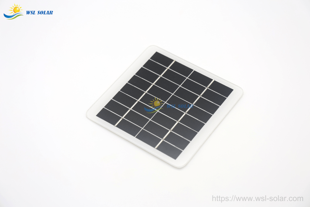
Key Features: – Utilize high efficiency mono PERC solar cell, up to 23% efficiency – Laminated by tempered glass, rigid, durable and long lasting – Waterproof, scratch resistant, and UV resistant – Customized solar panels for industrial use
Description: 2.5V 0.95W Solar Panel
This 0.95W solar panel utilizes high efficiency mono PERC solar cells with efficiency up to 23%, to ensure its high output. It is laminated by tempered glass to protect the solar cells inside, making it rigid, durable and long lasting. This tailor-made solar panel is waterproof, scratch resistant, and UV resistant, specially designed for long term outdoor use in any challenging condition.
Applications: Tempered glass solar panels are widely used in IoT applications, marine buoys, wireless sensors, traffic warning devise, GPS devices, asset tracking, electric fence chargers, outdoor lighting systems, weather monitoring systems etc.
The key to choosing between ETFE and PET lies in your intended use and duration: choose ETFE for long-term outdoor applications, and PET for short-term or indoor use.
While both are lightweight polymer materials, they differ significantly in performance and application. ETFE is a more modern and durable option, while PET is primarily geared towards scenarios where cost and lifespan are less critical.
solar calculators, solar lawn lights, low-power power banks, children’s toys, and other indoor or short-term outdoor electronic products
How to choose? 1. Choose ETFE If: You need durability: ETFE is self-cleaning, corrosion-resistant, and withstands harsh environments. It’s a permanent installation: Excellent for boats, RV roofs, or off-grid locations where you won’t replace panels often. You want higher efficiency: Higher transparency
2. Choose PET If: You are on a tight budget: PET panels are much cheaper to purchase. It’s for temporary use: Ideal for short-term camping, hiking, or portable charging. Storage is easy: Since they won’t last long outdoors, they are fine if used occasionally and stored indoors.
Critical Considerations Lifespan & Degradation: PET, being a plastic film, will become brittle and hazy, often developing a “milky” appearance after 0.5–2 years. Performance: ETFE surfaces are textured to catch more light, offering better efficiency in lower light conditions. Safety: PET panels are less thermally stable compared to the high-heat resistance of ETFE.
Summary: choose ETFE solar panels for long-term, permanent, or harsh outdoor installations (7–10 year lifespan) due to superior durability, high transparency (95%), and self-cleaning properties. Choose PET solar panels for budget-friendly, temporary, or portable uses (1–3 year lifespan), as they are cheaper but less UV-resistant and durable.
WSL Solar has been a quality and professional manufacturer of custom solar panels, solar mini panels, IoT solar panels and solar solution provider in China since 2006. Email: info@wsl-solar.com
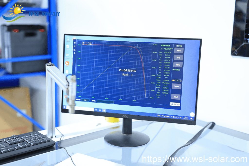
WSL Solar continuously introduces industry-leading production and testing equipment – this not only significantly improves production efficiency but also ensures that every product possesses highly consistent and superior performance. It is this dedication to quality and technology that allows us to consistently deliver high-quality, high-efficiency customized solar panels, while providing reliable solar solutions, earning the trust of a growing number of customers.
Choosing WSL Solar means choosing high efficiency, stability, and long-term value. Welcome to contact us for high quality custom solar panels.
WSL Solar has been a quality and professional manufacturer of custom solar panels, solar mini panels, IoT solar panels and solar solution provider in China since 2006.
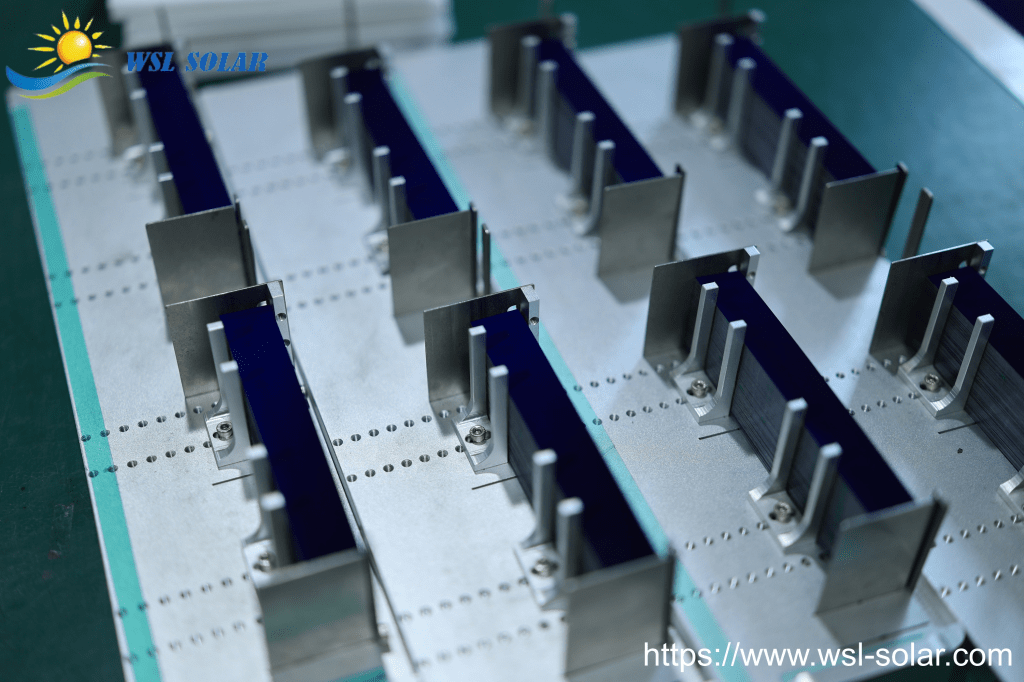
The core of the surface mount technology (SMT) manufacturing process for back contact (BC) solar panels lies in transferring all the main grid lines, originally located on the front, to the back, using a PCB (printed circuit board)-like process to achieve stress-free interconnection of the solar cells.
This process mainly consists of the following key steps, its ingenuity lying in replacing traditional solder ribbons with conductive backplates and conductive adhesive.
Working Principle and Core Steps
1. Prefabricated Conductive Backplate (equivalent to a “PCB” in SMT) Principle: In SMT, electronic components are mounted on a pre-fabricated PCB circuit board. Similarly, manufacturers prefabricate a “conductive backplate,” an insulating board with specific copper foil circuitry. Function: The circuitry on this backplate precisely corresponds to the positive and negative terminals on the back of each solar cell. It not only conducts electricity but also provides structural support for the entire assembly.
2. Precise Placement of Solar Cells (equivalent to “SMT placement”) Principle: This is consistent with the logic of an SMT placement machine precisely placing components onto pads. Using high-precision automated equipment, the back-contact solar cells are attached to their corresponding positions on the conductive backsheet according to a pre-designed spacing. Advantages: Because all electrodes are placed back-side down, there is no obstruction on the front, completely eliminating the 2%-3% light loss caused by the front-side main grid lines of traditional cells. This not only improves efficiency but also makes the module appearance more uniform and aesthetically pleasing.
3. Conductive Interconnection (equivalent to “reflow soldering” in SMT) Principle: This is the core technology, using conductive adhesive (ICA) or anisotropic conductive adhesive (ACA) instead of traditional high-temperature soldering. Process: The conductive adhesive is applied between the electrodes of the solar cell and the backsheet circuitry through printing or dispensing. Then, it is simultaneously heated and pressurized in a laminator, where the conductive adhesive cures under hot-press conditions, forming a stable and flexible electrical connection. Significant advantages: Traditional high-temperature soldering is prone to microcracks due to thermal stress, while this low-temperature conductive adhesive process has almost zero stress, allowing the use of thinner silicon wafers (down to 180 micrometers) and significantly improving the long-term reliability of components.
4. Integrated Encapsulation Principle: The stacked “glass – encapsulating film (EVA/POE) – interconnected solar cells and backsheet” are fed into a laminator. Under vacuum and high temperature, the encapsulating film melts and bonds all materials tightly together to form the final solar module.
Why choose SMT technology instead of traditional soldering?
The performance improvement brought by this process is revolutionary. Its main advantages are:
Features
Traditional solder ribbon process
SMT conductive backplane process
Shading Loss
Front main busbars block approximately 3% of sunlight
Zero shading, all electrodes are located on the back, maximizing the light-receiving area
Stress and Microcracks
High-temperature soldering causes high stress, easily leading to microcracks.
Stress-free connection significantly reduces breakage rate and microcrack risk.
Appearance
Visible silver-white solder ribbon
All-black/solid color, neat and aesthetically pleasing.
Series Resistance
Higher resistance at solder ribbon connection points
Lower contact resistance, higher conductivity, and higher module power
Wafer Thickness
Limited by the soldering process, cannot be too thin.
Compatible with ultra-thin wafers (<180µm), further reducing costs
Through this innovative interconnection method, back-contact technology not only achieves higher photoelectric conversion efficiency but also endows photovoltaic modules with stronger mechanical properties and a better appearance, making it one of the mainstream technologies for high-efficiency photovoltaic modules.
WSL Solar has been a quality and professional manufacturer of custom solar panels, solar mini panels, IoT solar panels and solar solution provider in China since 2006.
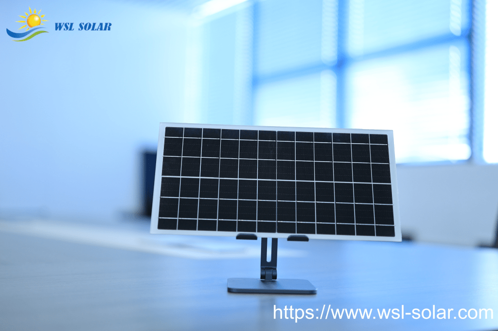
Key Features: – Utilize high efficiency mono PERC solar cell, up to 23.5% efficiency – Laminated by tempered glass, rigid, durable and long lasting – Waterproof, scratch resistant, and UV resistant – Customized solar panels for industrial use
Description: 9V 2.3W Solar Panel
This 2.3W solar panel utilizes high efficiency mono PERC solar cells with efficiency up to 23.5%, to ensure its high output. It is laminated by tempered glass to protect the solar cells inside, making it rigid, durable and long lasting. This tailor-made solar panel is waterproof, scratch resistant, and UV resistant, specially designed for long term outdoor use in any challenging condition.
Applications: Tempered glass solar panels are widely used in IoT applications, marine buoys, wireless sensors, traffic warning devise, GPS devices, asset tracking, electric fence chargers, outdoor lighting systems, weather monitoring systems etc.
Solar panels are composed of several materials, each playing a crucial role in the panel’s functionality, durability, and efficiency. Here are the primary materials used in the construction of solar panels:
1. Photovoltaic (PV) Cells: – Silicon: The most common material for PV cells. It can be monocrystalline, polycrystalline, or amorphous. – Cadmium Telluride (CdTe): Used in thin-film solar panels. – Copper Indium Gallium Selenide (CIGS): Another material used in thin-film solar panels. – Perovskite: An emerging material with high potential efficiency, still under research and development.
2. Encapsulation Material: – Ethylene-Vinyl Acetate (EVA): A transparent polymer that encapsulates the PV cells, protecting them from moisture and mechanical damage.
3. Backsheet: – Polymer Films: Typically made from materials like Tedlar (PVF), polyester, or polyvinyl fluoride (PVDF). The backsheet provides electrical insulation and protects the back of the panel from environmental factors.
4. Frame: – Aluminum: The most common material for the frame due to its lightweight, durability, and resistance to corrosion. The frame provides structural support and facilitates mounting.
5. Glass Cover: – Tempered Glass: High-strength, low-iron tempered glass is used as the front cover. It protects the PV cells from physical damage and environmental factors while allowing maximum light transmission.
6. Junction Box: – Plastic and Metal: The junction box is typically made from durable plastics and contains metal connectors. It houses the electrical connections and provides a safe interface for wiring.
7. Interconnectors: – Copper or Silver: These materials are used for the thin strips that connect individual solar cells within the panel, facilitating the flow of electricity.
8. Adhesives and Sealants: – Silicone and Other Polymers: Used to bond different layers of the solar panel together and to seal edges, ensuring durability and protection against moisture ingress.
9. Anti-Reflective Coating: – Silicon Nitride or Titanium Dioxide: Applied to the surface of the glass to reduce reflection and increase light absorption by the PV cells.
Summary of Material Functions: – PV Cells: Convert sunlight into electricity. – EVA Encapsulation: Protects cells and ensures durability. – Backsheet: Provides electrical insulation and environmental protection. – Frame: Offers structural support and facilitates installation. – Glass Cover: Protects the panel and maximizes light transmission. – Junction Box: Houses electrical connections. – Interconnectors: Facilitate electrical flow between cells. – Adhesives and Sealants: Ensure panel integrity and protection. – Anti-Reflective Coating: Enhances light absorption.
These materials work together to ensure that solar panels are efficient, durable, and capable of withstanding various environmental conditions over their lifespan.
Posted by Carrie Wong / WSL Solar WSL Solar has been a quality and professional manufacturer of custom solar panels, solar mini panels, IoT solar panels and solar solution provider in China since 2006. https://www.wsl-solar.com
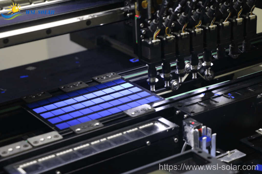
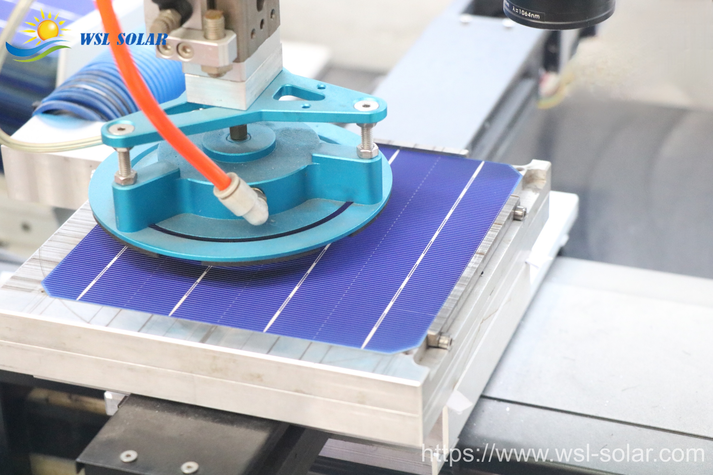
How laser cutting machine works to cut solar cells into small pieces according to your solar panel design?
Cutting solar cells into small pieces is a critical process in solar panel manufacturing, especially for high-efficiency custom solar panels with specific designs. Here’s a detailed breakdown of how laser cutting works for solar cells.
The Core Principle: Controlled-Fracture Cleaving (for Monocrystalline Cells)
The most common method doesn’t “burn” through the silicon like a traditional laser cutter might with metal. Instead, it uses a highly focused, low-power laser to create a controlled thermal stress that induces a perfectly clean split along the crystal lattice. This is known as “laser scribing and cleaving” or “laser thermal separation.”
Step-by-Step Process
1. Design & Programming
Your solar panel design is translated into a cutting path by CAD/CAM software.
The software accounts for the wafer’s thickness, material properties, and the required edge quality to minimize electrical losses.
2. Laser Scribing (The Key Step)
A short-pulse, low-power infrared (IR) laser is focused to an extremely fine spot on the surface of the silicon wafer.
The laser rapidly heats a tiny, localized volume of silicon (to over 1000°C) along the desired cut line.
This creates micro-cracks or modifies the material structure along a precise, shallow path (the “scribe line”). The depth is carefully controlled – typically only 10-30% of the wafer’s thickness.
Crucially, the laser does NOT vaporize the material. It creates internal stress and a weakened zone.
3. Cleaving / Breaking
After scribing, a mechanical breaking step is often used.
A controlled bending force applies pressure along the scribe line.
Due to the induced stress and the guided micro-cracks, the silicon wafer fractures perfectly along the laser-defined path, following its crystalline structure.
This results in a clean, smooth edge with minimal micro-cracks and no thermal damage zone (HAZ) that would reduce cell efficiency.
Why Laser Cutting is Superior for Solar Cells (Compared to Mechanical Saws)
Feature
Laser Scribing & Cleaving
Mechanical Diamond Saw/Scribing
Material Loss (Kerf)
Minimal (only the laser scribe line). Saves expensive silicon.
Significant (the width of the diamond blade). Wastes material.
Edge Quality
Very clean, smooth, low micro-crack depth. Higher mechanical strength.
Rougher, more micro-cracks, weaker edges prone to chipping.
Precision & Flexibility
Extremely high. Can cut complex shapes, curves, and very small shingles easily.
Low flexibility, typically only straight lines.
Throughput & Speed
Very high speed (meters per second). Non-contact process.
Slower, mechanical wear on blades.
Dust & Contamination
Almost none for the scribing step. Clean process.
Generates silicon slurry/dust that must be cleaned, causing contamination.
Thin Wafer Handling
Excellent. The only viable method for wafers <150μm thick without breakage.
High breakage rates on very thin wafers.
Critical Requirements for the Laser Process
Ultra-Precision: Cutting must be accurate to within microns to ensure cells are identical for automated stringing.
Minimal Heat Affected Zone (HAZ): The laser must not overheat the silicon, as heat creates defects that trap electrons, killing cell efficiency.
Strength Preservation: The cut edge must remain strong to survive the subsequent manufacturing processes (transport, stringing, lamination).
Summary In essence, a solar cell laser cutting machine uses a low-power, focused laser to “guide” a fracture through the crystalline silicon, rather than melting its way through. This cold-cutting process maximizes material yield, preserves the electrical quality of the silicon, and enables the intricate cell designs needed for today’s high-efficiency, high-power solar panels. It is an enabling technology for the continuous improvement in solar panel performance and cost-effectiveness.
Posted by Carrie Wong / WSL Solar WSL Solar has been a quality and professional manufacturer of custom solar panels, solar mini panels, IoT solar panels and solar solution provider in China since 2006. https://www.wsl-solar.com