The core of the surface mount technology (SMT) manufacturing process for back contact (BC) solar panels lies in transferring all the main grid lines, originally located on the front, to the back, using a PCB (printed circuit board)-like process to achieve stress-free interconnection of the solar cells.
This process mainly consists of the following key steps, its ingenuity lying in replacing traditional solder ribbons with conductive backplates and conductive adhesive.
Working Principle and Core Steps
1. Prefabricated Conductive Backplate (equivalent to a “PCB” in SMT)
Principle: In SMT, electronic components are mounted on a pre-fabricated PCB circuit board. Similarly, manufacturers prefabricate a “conductive backplate,” an insulating board with specific copper foil circuitry.
Function: The circuitry on this backplate precisely corresponds to the positive and negative terminals on the back of each solar cell. It not only conducts electricity but also provides structural support for the entire assembly.
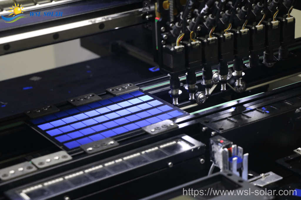
2. Precise Placement of Solar Cells (equivalent to “SMT placement”)
Principle: This is consistent with the logic of an SMT placement machine precisely placing components onto pads. Using high-precision automated equipment, the back-contact solar cells are attached to their corresponding positions on the conductive backsheet according to a pre-designed spacing.
Advantages: Because all electrodes are placed back-side down, there is no obstruction on the front, completely eliminating the 2%-3% light loss caused by the front-side main grid lines of traditional cells. This not only improves efficiency but also makes the module appearance more uniform and aesthetically pleasing.
3. Conductive Interconnection (equivalent to “reflow soldering” in SMT)
Principle: This is the core technology, using conductive adhesive (ICA) or anisotropic conductive adhesive (ACA) instead of traditional high-temperature soldering.
Process: The conductive adhesive is applied between the electrodes of the solar cell and the backsheet circuitry through printing or dispensing. Then, it is simultaneously heated and pressurized in a laminator, where the conductive adhesive cures under hot-press conditions, forming a stable and flexible electrical connection.
Significant advantages: Traditional high-temperature soldering is prone to microcracks due to thermal stress, while this low-temperature conductive adhesive process has almost zero stress, allowing the use of thinner silicon wafers (down to 180 micrometers) and significantly improving the long-term reliability of components.
4. Integrated Encapsulation
Principle: The stacked “glass – encapsulating film (EVA/POE) – interconnected solar cells and backsheet” are fed into a laminator. Under vacuum and high temperature, the encapsulating film melts and bonds all materials tightly together to form the final solar module.
Why choose SMT technology instead of traditional soldering?
The performance improvement brought by this process is revolutionary. Its main advantages are:
| Features | Traditional solder ribbon process | SMT conductive backplane process |
| Shading Loss | Front main busbars block approximately 3% of sunlight | Zero shading, all electrodes are located on the back, maximizing the light-receiving area |
| Stress and Microcracks | High-temperature soldering causes high stress, easily leading to microcracks. | Stress-free connection significantly reduces breakage rate and microcrack risk. |
| Appearance | Visible silver-white solder ribbon | All-black/solid color, neat and aesthetically pleasing. |
| Series Resistance | Higher resistance at solder ribbon connection points | Lower contact resistance, higher conductivity, and higher module power |
| Wafer Thickness | Limited by the soldering process, cannot be too thin. | Compatible with ultra-thin wafers (<180µm), further reducing costs |
Through this innovative interconnection method, back-contact technology not only achieves higher photoelectric conversion efficiency but also endows photovoltaic modules with stronger mechanical properties and a better appearance, making it one of the mainstream technologies for high-efficiency photovoltaic modules.
Posted by Carrie Wong / WSL Solar
WSL Solar has been a quality and professional manufacturer of custom solar panels, solar mini panels, IoT solar panels and solar solution provider in China since 2006.