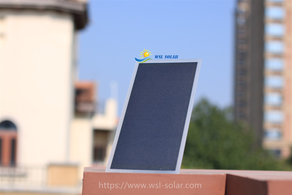
This 6v 1.2w IBC solar panel is built with the super high efficiency back contact solar cell (IBC solar cell). It is laminated by PET film, which is light weight and thin. This 6 volt solar panel is great for charging your 3.7-volt DC batteries and ideal for use in off grid applications such as IoT applications, wireless sensors etc.
Features: – IBC solar cell with efficiencies of up to 23% guarantee high power output – Matte finish and no busbar on panel surface – PET laminated, light weight and thin – Waterproof, scratch resistant & UV resistant – Excellent performance under low light environments – Custom manufacturing in various size & shapes available
PET Solar Panel means that the top layer of encapsulated material is PET film, which is a plastic film with a light transmittance of about 85%. Its surface can look shiny without any treatment, and if it is sprayed with a layer of frosted, it will look matte and a little rough to the touch.
PET solar panels are customized products with small sizes or low power output. The product structure is PET Film + EVA + Solar Cells + EVA or not + PCB. The solar cells are cut into small pieces by a laser machine, and the voltage and the electric current can be done as per the requirements, and then the single-layer transparent PET, EVA, solar cells, EVA, PCB backplanes are sequentially placed in a solar laminator for lamination. After about 20 minutes, take it out and then stick a soft and transparent protective film on the surface of the solar panel.
What are the advantages of PET solar panels? 1. It is suitable for the production of solar modules of various sizes and different voltages and currents to meet different application scenarios. 2. Quality standards are lower than glass laminated solar panel. 3. Short lamination time and high production efficiency. 4. Low cost.
What are the disadvantages of PET solar panels? 1. Long-term exposure to the outdoors will make the PET film hard, brittle, and discolored, reducing the light transmittance of the solar panel, and at the same time, it can’t well protect the PV cells inside to avoid oxidation and corrosion. If the surface is frosted, this layer of frosted will start to fall off and become very ugly after about 0.5 years. 2. Because the lamination time is not enough, the cross-linking degree of the entire solar panel will not meet the requirements. 3. It can’t resist the relatively large impact from the outside.
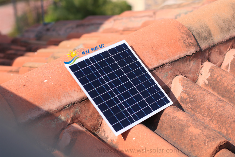
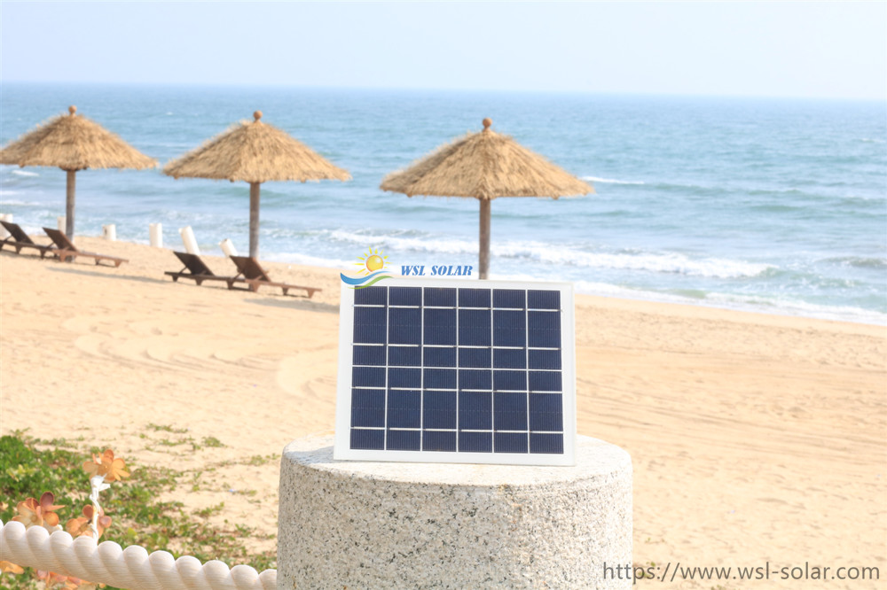
What are the applications of PET solar panels? Used for solar lawn lights, solar wall lights, solar handicrafts, solar toys, solar radios, solar flashlights, solar mobile phone chargers, solar small water pumps, solar home/office power supplies and portable mobile power systems and other products. It is not recommended to use PET solar panels that need to be placed outdoors for a long time and have a life expectancy of more than 2 years.
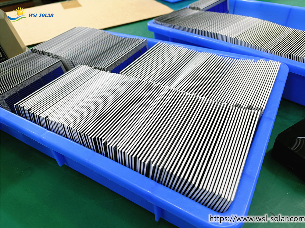
WSL Solar has been a quality and professional manufacturer of custom solar panels, solar mini panels, IoT solar panels and solar solution provider in China since 2006.
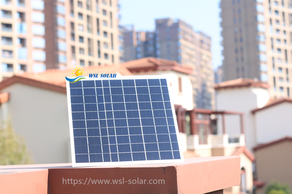
WSL Solar’s 2W 8V custom shaped solar panel is built with the latest high efficiency mono PERC solar cell. It is laminated by tempered glass, which is durable and robust. This black solar panel comes with a black back sheet, a matte black frame and black solar cells, providing an all-black aesthetic. This custom solar panel is ideal for use in off grid applications such as solar powered LED lighting, IoT solar, solar traffic sign, small solar powered system etc.
Features: – With latest high efficiency mono PERC solar cell – With black back sheet, matte black frame, providing all-black aesthetic – Positive power tolerance – Tempered glass laminated, high transmission,durable & robust – Withstanding challenging environmental conditions – Waterproof, scratch resistant & UV resistant
WSL Solar’s 4W 5V IoT solar panel is built with the latest monocrystalline PERC solar cell. It is laminated by tempered glass, which is durable and robust. This custom solar panel is ideal for use in off grid applications such as IoT devices, solar powered LED lightings, solar traffic signs, small solar powered systems etc.
Amorphous solar cell (or indoor solar cell) can harvest energy and generate electricity from environment light like sunlight or indoor light. It has good performance during weak light condition. This kind of solar cell can be used to power low-consumption electronic devices, such as wireless sensors, IoT devices, ETC devices, calculators etc.
Amorphous silicon solar cells are thin-film solar cells based on amorphous silicon compounds. According to different materials, current silicon solar cells can be divided into three categories: monocrystalline silicon solar cells, polycrystalline silicon thin film solar cells and amorphous silicon thin film solar cells.
Advantages of amorphous solar cells 1. Low production cost: Due to the low reaction temperature, it can be manufactured at a temperature of about 200 °C, so films can be deposited on glass, stainless steel plates, ceramic plates, and flexible plastic sheets, which are easy to produce in large areas and have low costs.
2. Short energy return period: Amorphous silicon solar cells with a conversion efficiency of 6% use about 1.9 kWh/W of electricity for production, and the time to return the above energy after generating electricity is only 1.5-2 years.
3. Suitable for mass production: Amorphous silicon material is formed by vapor deposition, and the commonly used method is plasma enhanced chemical vapor deposition (PECVD) method. This manufacturing process can be continuously completed in multiple vacuum deposition chambers, thereby realizing mass production. The main process (PECVD) of amorphous silicon solar cells using glass substrates is similar to that of TFT-LCD array production, and the production methods have the characteristics of high degree of automation and high production efficiency.
In terms of manufacturing methods, there are electron cyclotron resonance method, photochemical vapor deposition method, DC glow discharge method, radio frequency glow discharge method, sputtering method and hot wire method. In particular, the radio frequency glow discharge method has become an internationally recognized mature technology because of its low temperature process (~200 °C), which is easy to achieve large-scale and large-scale continuous production.
4. Good high temperature performance: when the working temperature of the solar cell is higher than the standard test temperature of 25 °C, its optimal output power will decrease; the temperature of the amorphous silicon solar cell is much less affected by the temperature than the crystalline silicon solar cell.
5. Good response to weak light and high charging efficiency: The absorption coefficient of amorphous silicon material is in the entire visible light range, and it has a good adaptability to low light and strong light in actual use.
The above-mentioned unique technical advantages make thin-film silicon cells have broad application prospects in the civilian field, such as photovoltaic building integration, large-scale low-cost power stations, and solar lighting sources.
Disadvantages of amorphous silicon solar cells The industry has had doubts about amorphous silicon thin-film solar cells before, mainly because of their low cell conversion efficiency (5%-9%), and extremely fast decay, with a limited service life of only 2-3 years.
With the advancement of technology, the current mainstream amorphous silicon thin film solar cells have a service life of more than 10 years. This makes amorphous silicon thin-film solar cells one of the most promising thin-film cell technologies at present.
WSL Solar has been a quality and professional manufacturer of custom solar panels, solar mini panels and solar solution provider in China since 2006. https://www.wsl-solar.com
WSL Solar has been a quality and professional manufacturer of customized solar panels and solar solution provider in China since 2006.
Using the latest solar technology, all solar panels are 100% inspected before shipment, strict quality control, honesty and trustworthiness, mutual benefit, these are what we have been doing.
We are very grateful to our customers for their trust and support over the years. WSL Solar will continue to provide high-efficiency customized solar panels, optimized solar solutions and high-quality services.
Silicon wafers are divided into semiconductor wafers and photovoltaic wafers according to their uses. Photovoltaic silicon wafers can be single crystal silicon or polycrystalline silicon, and semiconductor silicon wafers can only be single crystal silicon. The biggest difference between the two is that the content and purity of silicon are different. The conversion efficiency of monocrystalline silicon is generally about 18.5%~25%, and the conversion efficiency of polycrystalline silicon wafer is about 17.3%. Correspondingly, monocrystalline silicon solar cells have higher photoelectric conversion efficiency than polycrystalline silicon solar cells.
Over the years, the silicon wafer size has experienced a process from small to large. The increase in silicon wafer size and the continuous progress of photovoltaic technology have promoted the cost reduction and efficiency improvement of the entire photovoltaic industry chain.
For silicon wafer manufacturers, the larger size of silicon wafers can reduce the three major costs of silicon wafer companies: silicon material, crystal pulling, and slicing. The same amount of silicon material can reduce the number of crystal pulling and energy consumption when the diameter of the silicon rod becomes larger, thereby reducing the cost of crystal pulling. At the same time, large-sized silicon wafers can reduce the number of slices, the cost of slices and the cost per watt of silicon wafers.
For solar cell and solar panel manufacturers, the larger size of silicon wafers can speed up the production speed of silicon wafers to solar modules, which will also reduce production and operation costs such as manpower, water and electricity, and dilute the production process of solar cell modules. Non-silicon cost. As the size of a single silicon wafer increases, the number of cells in a single solar module decreases, the number of silicon wafers decreases accordingly, and the effective light-emitting area of the solar module increases, which will lead to an increase in conversion efficiency and power, and a decrease in the cost per watt. .
For power station customers, under the same power station scale, the larger the size of the solar modules, the less the number of solar modules required, thereby reducing the corresponding brackets, combiner boxes, cable costs, transportation and installation costs, etc. At the same time, large-sized silicon wafers will improve the power and quality of solar modules to a certain extent, and increase the power generation capacity of the power station while reducing the cost of the power station.
Under the driving force of diluting costs and improving the quality of solar modules, the silicon wafer size has grown from 100mm to 210mm in the past 40 years from 1981 to the present.
1981-2012: 100mm-156mm Between 1981 and 2012, silicon wafers had margins of 100mm and 125mm, and were dominated by 125mm silicon wafers. After that, the margin of silicon wafer was greatly increased from 125mm to 156mm (ie M0), an increase of 54.1%. 156mm silicon wafer has gradually become a popular choice for p-type monocrystalline and polycrystalline silicon wafers. Around 2014, 125mm P-type silicon wafers were basically eliminated and only used in some IBC and HIT battery modules.
2012-2018: M0-M2 At the end of 2013, several major manufacturers took the lead in unifying M1 (margin 156.75mm, diameter 205mm) and M2 (margin 156.75mm, diameter 210mm) silicon wafers with a standard of 156.75mm, which is a major change in the history of silicon wafer size development. . In 2017, the size standard was reviewed and approved by the SEMI standards committee. The revised version of the national standard for polysilicon wafers in 2018 also determined 156.75mm as the standard side length, and suggested that future size increases should be changed in multiples of 1mm.
2018 to present: M2—M6 Under the situation of increasing demand for high-power components, some manufacturers began to achieve this goal by increasing the area of the battery, resulting in the emergence of 157.0, 157.3, 157.5, 157.75, 158.0 and other silicon wafers in the market. The organization and management of the chain brings great inconvenience. After the melee, two mainstream sizes appeared on the market: G1 square monocrystalline (158.75mm margin) and M6 (166mm margin) large silicon wafers.
The ultimate in wafer size: 210mm In August 2019, Zhonghuan launched the G12 (210mm margin) large silicon wafer, which greatly increased the area of the M6 silicon wafer by 60.8%. According to the data, the cost of G12 cells is 25.56% lower than that of M2, and the cost of components is reduced by 16.8%.
The change in the size of silicon wafers over the past 40 years reflects the parity process of the entire industry. With the advent of the parity era, a new starting point for the photovoltaic industry has just begun.