The assembly process of a small, custom solar panel involves preparing the materials, electrically connecting the solar cells, encapsulating them for protection, framing the unit, and performing final testing.
Materials Needed
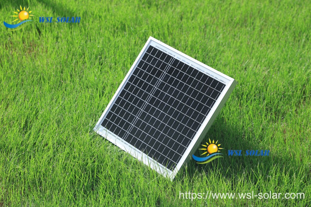
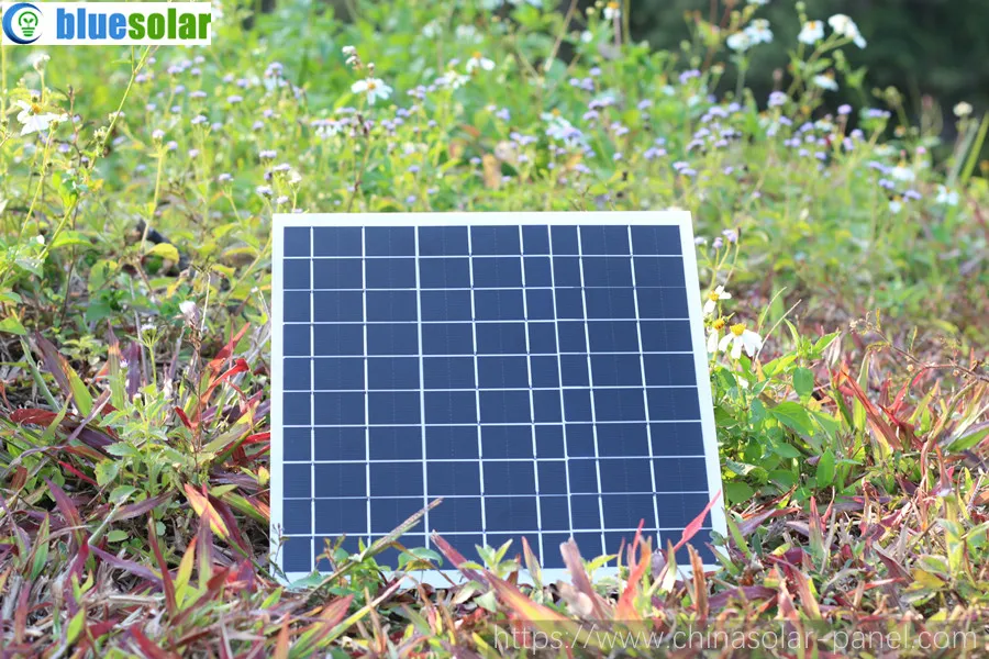
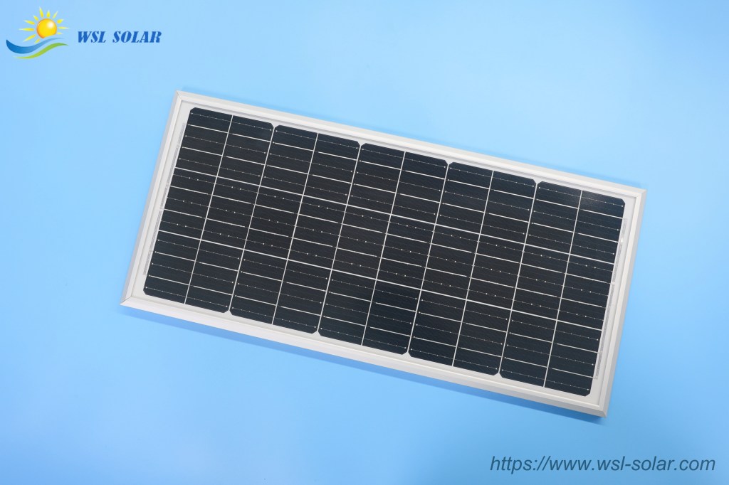
- Solar cells: The core components that convert light into electricity. Monocrystalline or polycrystalline, typically 0.5V each. The number determines the voltage (e.g., 36 cells for an ~18V panel).
- Encapsulant (EVA film): Ethylene Vinyl Acetate, a clear material that bonds and protects the cells. They become clear when heated.
- Cover (Tempered glass or clear plastic): Protects the front from weather and impact.
- Backsheet: A durable polymer layer on the back for insulation and moisture protection.
- Frame (Aluminum or wood): Provides structural integrity and a mounting point.
- Tabbing and bus wire: Flat, coated copper wires for electrical connections.
- Junction box: Houses the electrical connections and bypass diodes.
- Sealant (Silicone/Epoxy): Used for sealing edges and the junction box to prevent water intrusion.
- Soldering iron and solder: For making the electrical connections.
Assembly Steps
- Preparation and Template Creation: A template is created to ensure the correct and even placement of the solar cells on a backing board.
- Cell Stringing (Connecting Cells): Individual solar cells are connected in series (positive to negative) using tabbing wire and a soldering iron to achieve the desired voltage. The size of the cell determines the amperage, while the number of cells in series determines the voltage.
- Laying Up the Panel: The stack of materials is layered in the following order: glass, a layer of EVA film, the interconnected solar cells, a second layer of EVA film, and finally the backsheet.
- Bussing Soldering: The strings of cells are connected to each other using a thicker bus wire to form the complete electrical circuit.
- Lamination: The layered panel assembly is placed in a laminator (or sealed manually with even pressure and a clear cover) under vacuum and high temperature. This melts the EVA, encapsulating the cells and bonding all the layers together for durability and weather resistance.
- Trimming and Framing: Any excess encapsulant material around the edges is trimmed off. The laminated unit is then fitted into a protective aluminum or wooden frame.
- Junction Box Installation: A junction box is attached to the back of the panel and the main positive and negative output wires are connected to it. A blocking diode may be included here to prevent current backflow. The box and edges are sealed with silicone or epoxy.
- Testing and Quality Control: The finished panel undergoes electrical tests, such as a sun simulator test and an electroluminescence (EL) test, to measure its performance and check for any micro-cracks or defects.
- Final Steps: The panel is cleaned, labeled with its specifications, and packaged for use.
Posted by Carrie Wong / WSL Solar
WSL Solar has been a quality and professional manufacturer of custom solar panels, solar mini panels, IoT solar panels and solar solution provider in China since 2006.
https://www.wsl-solar.com